Tech Giants NVIDIA, ASML, TSMC, and Synopsys Collaborate to Revolutionize Chip Manufacturing for Next Generation
NVIDIA announces cuLitho, a breakthrough software library for computational lithography, integrated by industry leaders TSMC, Synopsys, and ASML to accelerate the design and manufacturing of next-generation chips.

SINGAPORE—GTC—March 22, 2023— NVIDIA has made a significant announcement that could revolutionize the field of computational lithography. The company has developed the new cuLitho software library, which will enable leading semiconductor manufacturers such as ASML, TSMC, and Synopsys to accelerate the design and manufacturing of next-generation chips.
With current production processes reaching their physical limits, the integration of cuLitho into software, manufacturing processes, and systems for the latest-generation NVIDIA Hopper™ architecture GPUs is expected to enable the production of chips with tinier transistors and wires while reducing the time to market and improving energy efficiency. This development is particularly crucial for massive data centers that run non-stop to power the manufacturing process. Additionally, ASML plans to integrate GPU support into all of its computational lithography software products.
“The chip industry is the foundation of nearly every other industry in the world,” said Jensen Huang, founder and CEO of NVIDIA. “With lithography at the limits of physics, NVIDIA’s introduction of cuLitho and collaboration with our partners TSMC, ASML and Synopsys allows fabs to increase throughput, reduce their carbon footprint and set the foundation for 2nm and beyond.”
Running on GPUs, cuLitho has achieved a remarkable performance leap of up to 40 times faster than current lithography, which involves creating patterns on a silicon wafer. This breakthrough enables the acceleration of the massive computational workloads that consume tens of billions of CPU hours every year. With cuLitho, 500 NVIDIA DGX H100 systems can perform the work of 40,000 CPU systems by running all parts of the computational lithography process in parallel. This helps to reduce power consumption and minimize environmental impact.
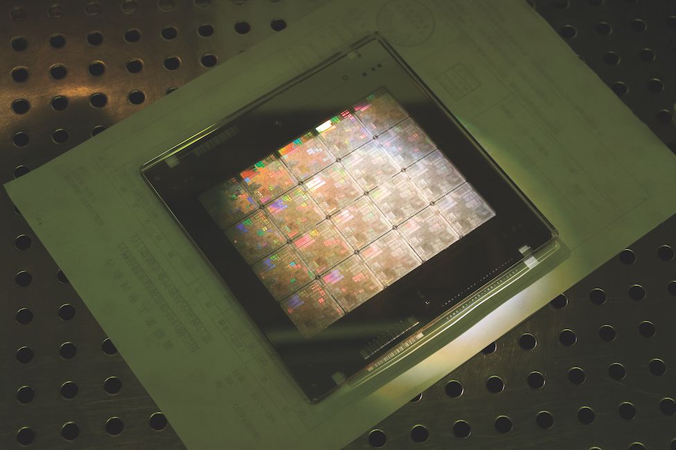
In the short term, fabs using cuLitho could produce 3-5 times more photomasks, which are the templates for a chip’s design, using only 9 times less power than current configurations. Furthermore, a photomask that previously took two weeks to process can now be completed overnight.
Adoption and Support by Industry Leaders
NVIDIA is working with key partners to smooth the speedy adoption of these new technologies.
“The cuLitho team has made admirable progress on speeding up computational lithography by moving expensive operations to GPU,” said C.C. Wei, CEO of TSMC. “This development opens up new possibilities for TSMC to deploy lithography solutions like inverse lithography technology and deep learning more broadly in chip manufacturing, making important contributions to the continuation of semiconductor scaling.”
“We are planning to integrate support for GPUs into all of our computational lithography software products,” said Peter Wennink, CEO of ASML. “Our collaboration with NVIDIA on GPUs and cuLitho should result in tremendous benefit to computational lithography, and therefore to semiconductor scaling. This will be especially true in the era of high NA extreme ultraviolet lithography.”
“Computational lithography, specifically optical proximity correction, or OPC, is pushing the boundaries of compute workloads for the most advanced chips,” said Aart de Geus, chair and CEO of Synopsys. “By collaborating with our partner NVIDIA to run Synopsys OPC software on the cuLitho platform, we massively accelerated the performance from weeks to days! The team-up of our two leading companies continues to force amazing advances in the industry."
Looking ahead, cuLitho is poised to enable better design rules, higher density, higher yields, and AI-powered lithography.
Revolutionizing Semiconductor Scaling
With the growing number of transistors in newer nodes and more stringent accuracy requirements, the computational time needed for the largest workloads in semiconductor manufacturing has been outpacing Moore’s law. This has slowed down the pace of innovation in the industry as future nodes require more detailed calculations that cannot fit into the available computational bandwidth provided by current platforms. Additionally, fab process changes often require an OPC revision, leading to bottlenecks. The introduction of cuLitho not only helps eliminate these bottlenecks but also opens up the possibility of novel solutions and innovative techniques such as curvilinear masks, high NA EUV lithography, and sub-atomic photoresist modeling that are necessary for new technology nodes.
To learn more, watch the GTC 2023 keynote from Huang and attend the conference session “Accelerating Computational Lithography” presented by NVIDIA cuLitho architect Vivek K. Singh. Registration for GTC is free.


